Assembly Technologies
Any chip, produced by a wafer process in the semiconductor industry, has to be assembled in a device and/or a modul before it can carry on function. For that purpose conductive, stable and very reliable connections between the pads of the chip and the external leads (first level interconnects) and continuing in the package and onto the next interconnection level of modules (second level interconncects) are needed.
The electronics packaging permanently opens up new applications and special solutions beside the mainstream processes of bonding, soldering or conductive adhesive bonding on rigid organic, flexible organic or inorganic substrates. The diversification of component packages, the further development of substrate and interconnecting materials and the specific operational conditions for electronic products lead to special adapted technologies. The field of activity “assembly technologies” is focused on the modification of standard technologies as well as on the development of new ones.
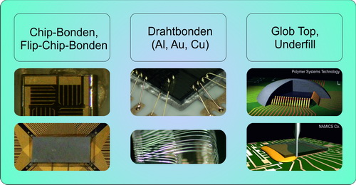
In more than 80% of all applications now and in the foreseeable future these connections are realized by Chip and Wire Bonding. As a rule the back side of the chips is bonded with adhesive on a substrate or housing. The electrical interconnections from the chip are realized by micro wires with diameters down to 20µm, which are welded with their respective connection areas.
The Flip Chip Technology allows connecting the front side of the chips directly on the substrate. For this, special bumps are applied on the pads to ensure a stable and reliable interconnection. Typically, Adhesive and Soldering Technologies are chosen to realize the interconnection. In the field of microjoining technology, materials and technologies are to be analyzed and characterized for processing the semiconductor chips to devices or modules. The aim is the miniaturization and the increasing of the reliability. One core topic is the field of Wire Bonding. We investigate the ability of different innovative materials for the wire on different materials for the surface finishing.
Using nanotechnologies in the semiconductor manufacturing are leading to a rapid increase of the number of elements and/or transistors on the chip. Beside many other changes this fact results in a significant increase of the number of pads per chip. Therefore for inter connecting in the future only very small pads both on the chip and the substrates or the leadframes will be available. Consequently an extremely miniaturization is going on. Especially with regard to Wire bonding this has influence to the used wires as well as the bonding process. The top requirement for all time remains the reliability of the contacts, which has to be guaranteed by using the results of scientific material investigations and by stable conditions during the whole production process. All considerations about trends in materials and technologies for microjoining aim in that direction, and from our Laboratory together with the packaging industry a roadmap for microjoining technologies was created considering these ideas.

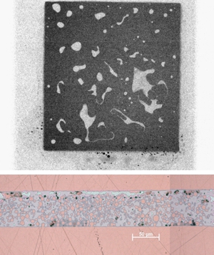
Surface Mount Technology today has to face a wide range of different demands. Those are dictated by the product requirements, operational conditions of the later electronics modules and reliability demands. This leads in consequence to a diversification of packaging technologies. Beside the "traditional" interconnect technologies like soldering and conductive adhesive bonding technologies are modified (e.g. the diffusion soldering) soldering in combination with presure variations to get mor homogeneous area solder joints for power semiconductors as well as new technologies like sintering.
Diffusion soldering, as one example, offers the opportunity to build interconnections by isothermal solidification at same temperature levels of some 250°C as used for reflow soldering of SnAgCu alloys. At the same time such interconnections, if the intermetallic compound is formed through the whole connection, after solidification can survive temperature loads of 400°C and more. This is a very important feature with regard to power electronic modules with extreme current densities. However, the relibility behaviour of the whole package changes too and has to be completely evaluated again.