Public funded research projects at IAVT/ZmP
TU Dresden - Chair of Process Diagnostics for Energy and Process Engineering
TU Dresden - Chair of Hydrogen and Nuclear Energy
FAU Erlangen-Nuremberg
Helmholtz-Center Dresden-Rossendorf
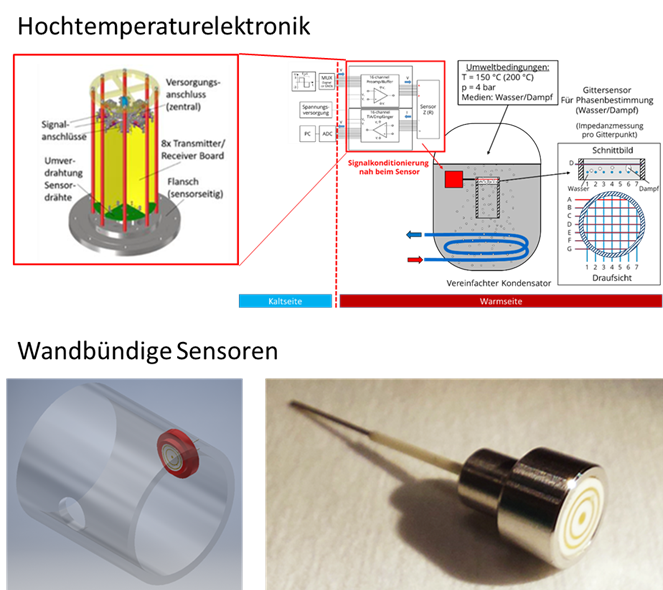
The ROBINIE project focuses on developing and qualifying robust electrical measurement techniques to capture thermohydraulic processes in large-scale test facilities (TOPFLOW, THAI, SECA) with high temporal and spatial resolution. The aim is to clarify key safety issues through experimental studies—particularly regarding passive emergency cooling systems and two-phase flows. The IAVT is involved in specific sub-projects within two work packages.
Work Package 1 focuses on the development and deployment of a wire-mesh sensor equipped with specialized high-temperature electronics. The primary emphasis is on the design and evaluation of the electronics and a pressure-resistant housing concept. The sensor is used in containment test facilities operated by the partner Becker Technologies to conduct detailed investigations of two-phase flows.
Work Package 2 covers the fabrication and qualification of flush-mounted sensors for measuring film thickness during wall condensation. The focus here is on robustness and performance analysis under thermal stress.
- Fraunhofer IIS, Inst.-Teil Entwicklung Adaptiver Systeme IIS/EAS (Koordinator)
- Hochschule für Technik und Wirtschaft Dresden HTWD
- Technische Universität Chemnitz TUC
- Fraunhofer ENAS
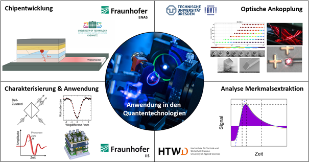
Quantum technologies are becoming increasingly important for the economy and society, for example through the increased performance of quantum computers, secure communication using quantum key distribution, and precise measurements using quantum sensors. Current light sources such as lasers can only be controlled to a limited extent at the single-photon level. The only alternatives that can reliably emit single photons are individual atoms, molecules, or quantum dots (QD). Inorganic quantum dots offer the advantage of acting as stable and controllable photon sources, as they are easier to handle than atoms and less susceptible to instabilities than molecules. The research focus of the project is in the field of deterministic photon sources. Fundamental research focuses on their performance, controllability, and miniaturization to enable the universal use of these systems in future applications. In this context, our institute (TUD-IAVT) is working on the development of photonic packaging for the integration of QD light sources. The subject of the investigations is the technology development for the fabrication of novel optical integrated redistribution substrates based on planar single-mode optical waveguides and micro-coupling optical components (lenses, mirrors).
- Fraunhofer IPA
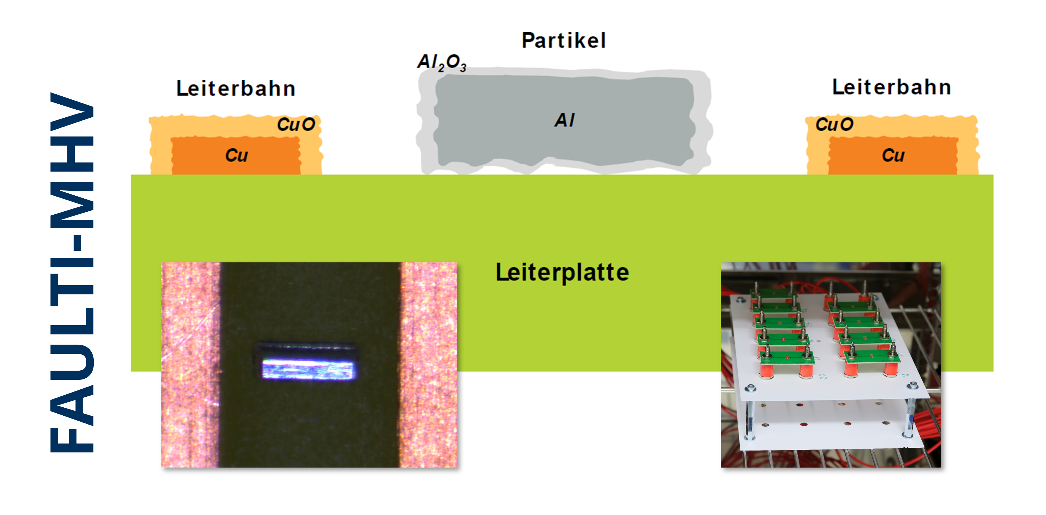
Particle contamination in high-voltage modules for automotive applications poses a functional and safety risk that is currently difficult to assess. DIN EN IEC 60664-1:2022 is frequently applied in the context of insulation coordination, but this standard is limited to contamination of the "micro-environment." It is currently unclear how macroscopic contamination of the module surface or contamination of the macro-environment of the module surface, as addressed in the ZVEI guideline "Technical Cleanliness in Electrical Engineering" and its international counterpart IEC TR 61191-7:2020, should be considered when designing clearances and creepage distances. Furthermore, the risks posed by, for example, textile fibers or plastic particles under the influence of moisture and heat are unknown.
It is also unclear what risks arise from these particles. To answer these questions, the Federal Ministry of Education and Research (BMBF, now BMFTR), with the participation of co-financing industry partners (e.g., Aptiv, BMW, Bosch, Continental), initiated the "FAULTI-MHV" project. The project aims to develop and test various methods and test benches to conduct experiments answering the questions mentioned above.
- Wrocław University of Science and Technology (WUST)
- University of Žilina (UNIZA)
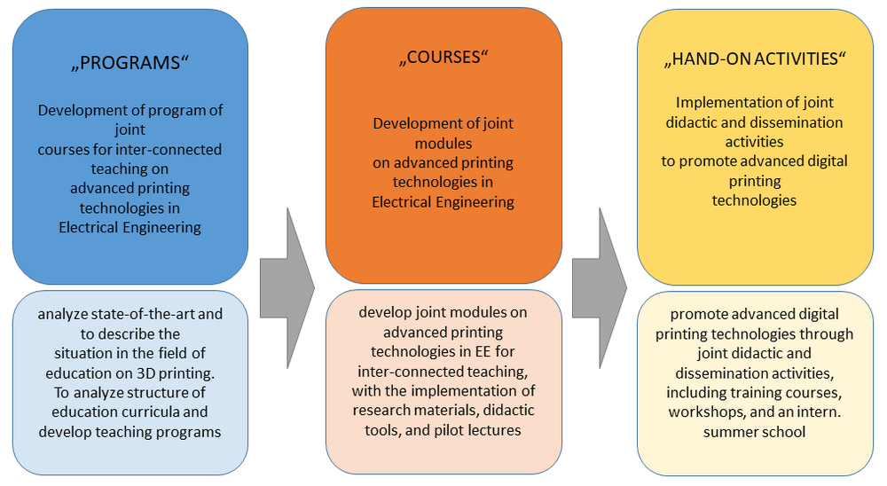
Our project centers around introducing advanced printing technologies (APT) into university education. The project aims to advocate for the use of digital additive manufacturing (DAM) technologies in teaching, especially design methods and printing technologies. DAM has a uniquely short timespan from initial idea over design process to actual manufacturing and can be utilized in some form at any university. This allows students to get direct feedback and hands-on knowledge even tough multiple iterations, without the enormous time and investment needed for traditional micro technologies. From our experience in teaching, ways to connect theory and praxis are few but urgently needed to train holistic and enthusiastic engineers and scientist. We see 3D micro printing as a way achieve the goal to shorten the arrival of scientific innovations in academic teaching. TADAM project is utilized in 3 phases, each involving students and academic staff from all partner universities (see picture).
- TU Dresden:
- Institut für Halbleiter- und Mikrosystemtechnik, IHM (Koordinator)
- Institut für Aufbau- und Verbindungstechnik, IAVT
- Faculty of Medicine Carl Gustav Carus, Medical Clinic 1
- Ovesco Endoscopy AG
- Renesas Germany GmbH (associated partner)
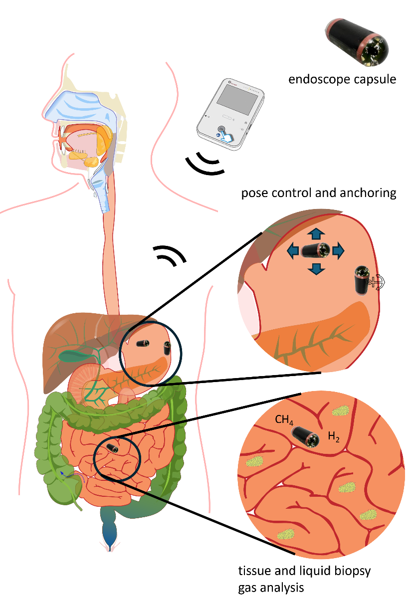
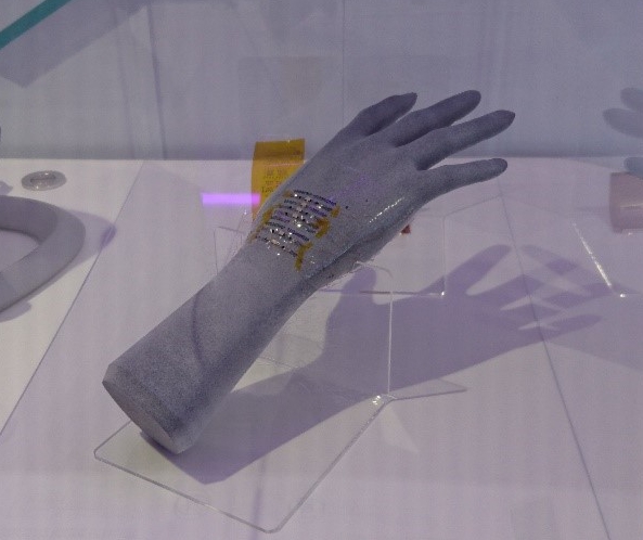
SEMECO-A4, Active intelligent capsule endoscopy
In Germany, around 6 million endoscopies are performed every year. They play a central role in the diagnosis and treatment of cancer and other diseases of the gastrointestinal tract. Capsule endoscopes are an attractive alternative to traditional diagnostic procedures, as they offer a diagnosis of the entire gastrointestinal tract with reduced discomfort or risk of injury for the patient. In addition, regions of the small intestines can be reached that are not accessible by traditional endoscopy. Capsule endoscopes have the potential to significantly reduce the workload of gastroenterologists. Our vision is to develop enhanced functions for capsule endoscopes that include gas sensors and adaptive anchoring mechanisms, the ability to take tissue and liquid biopsies and in vivo microbiome analysis using gas sensors. In addition, secure bidirectional communication through the body at high data rates must be guaranteed. Magnetic capsule pose control will facilitate the precise actuation of the developed mechanisms. Our vision is to develop enhanced functions for capsule endoscopes that include adaptive anchoring mechanisms, the ability to take tissue and liquid biopsies and in vivo microbiome analysis using gas sensors. In addition, secure bidirectional communication through the body at high data rates must be guaranteed. Magnetic capsule pose control will facilitate the precise actuation of the developed mechanisms.
TUD Institute for Mechatronic Mechanical Engineering, Endowed Professorship for Construction Machinery
Electrical assemblies are being installed in increasing numbers and with growing integration into construction machinery due to the increasing automation, digitalization, and electrification of construction sites and their equipment. These assemblies, especially in construction machinery and its attachments, are often exposed to severe thermal and mechanical stresses. A significant problem is that many electrical components are not designed or dimensioned for such stresses. Furthermore, no standard for testing electronics in construction site environments exists. This problem leads to the following objectives:
- Recording and evaluating operating loads on construction machinery
- Analyzing complex assemblies in use
- Developing a method for testing electrical assemblies and/or components for use in construction machinery
- Deriving recommendations for the development of electrical assemblies for construction machinery
- Technische Universität Dresden
- Vodafone Chair of Mobile Communications Systems
- Institute of Electronic Packaging Technology
- Chair of Compiler Construction
- Chair of Circuit Design and Network Theory
- Chair of Radio Frequency and Photonics Engineering
- eesy-IC GmbH Erlangen
- ficonTEC Service GmbH Achim
- viimagic GmbH Dresden
- GCD Printlayout GmbH Erlangen
- Micro Systems Engineering GmbH Berg/Ofr.
- VI-Systems GmbH Berlin
- Associated: GlobalFoundries LLC & Co. KG, Nokia Bell Labs, Vodafone GmbH, Cloud&Heat Technologies GmbH, National Instruments Corp.
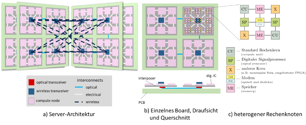
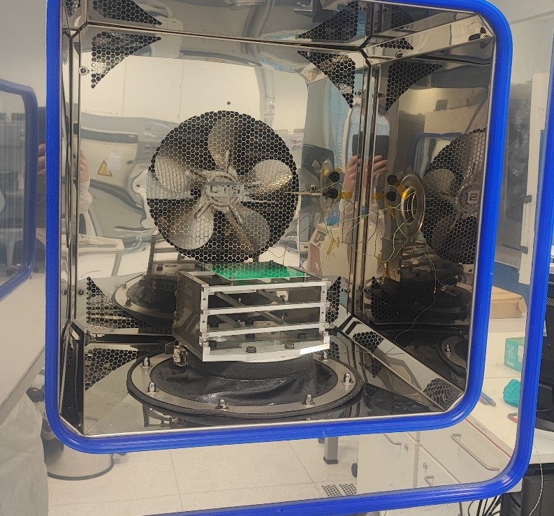
The BMBF project E4C (Extrem Energieeffiziente Edge Cloud Hardware am Beispiel Cloud Radio Access Network) develops an innovative concept for new, scalable computer architecture, which combines the specialized computing nodes and a new data communication structure based on electrical, optical and wireless communication links. This architecture can be implemented into edge-servers in virtualized 5G mobile access networks and can have a capability for energy saving up to 90%. The fabrication of such heterogeneous computing node (see figure) needs a co-integration of chip components on a common interposer substrate. Our institute will in the E4C-project work on packaging approaches for integration and of optical and wireless transceivers (TRx). The DFG CRC 912 HAEC explored on scalable fabrication methods for the integration of optical and mm-wave hardware. Based on this experience, in this project passive components (optical couplers, antennas etc.) will be co-integrated with active ICs into the TRx-packages. The E4C-targeted energy saving will be pursued in the packaging field by using of low-loss and reliable contacts and optimized wiring as well as with application of novel chip integration technologies.
The E4C-project proposes an innovative hardware approach to solve a key problem of 5G-base stations, which in future will bear a significant energy costs for the distribution of computing load in virtualized mobile access networks.
IMG Electronic & Power Systems GmbH
budatec GmbH
PFARR Stanztechnik GmbH
G&W Leiterplatten Dresden GmbH & Co. KG
Fraunhofer IKTS, Materialdiagnostik
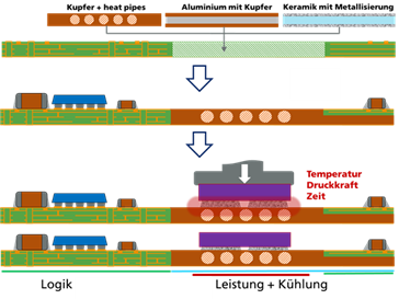
The goal of this project is the first-ever integration of hybrid printed circuit boards with the connection technologies diffusion soldering, sintering and SMT soldering through heterogeneous
integration, in order to enable SMEs to produce highly integrated modules of high-performance electronics from 20 kW upwards. Using the exemplary functional assembly from the application provider IMG (railway electronics, Line 10 Nordhausen, approx. 180 kW), consisting of power electronic inverters and control electronics, the following objectives will be pursued and technologically demonstrated:
- first-time integration of high-current printed circuit boards and selective temperature-resistant joining technology,
- multiple functional elements integrated into the printed circuit board (see heat pipe),
- first-time integrated solution of logic and power sections on a single assembly as a "single-board unit" within power electronics,
- cost reduction in the manufacturing of power electronics, and
- increased power density for power electronics in the range from 20 kW to 200 kW and above through reduced installation space and weight.
eologix sensor technology GmbH (Österreich)
SES-TEC OG (Österreich)
FH JOANNEUM GmbH, Institut Electronic Engineering (Österreich)
Universität Klagenfurt, Institut für Intelligente Sensorsysteme (Österreich)
LFG Oertel e.K. (Deutschland)
STV Electronic GmbH (Deutschland)
Technische Universität Berlin, Forschungsschwerpunkt Technologien der Mikroperipherik (Deutschland)
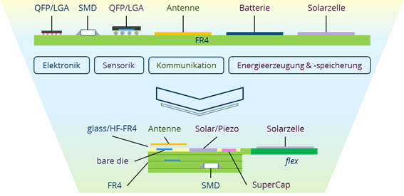
Monitoring efficiency-sensitive and safety-critical systems requires new electronic sensor modules with improved functionality, integrability, reliability, and manufacturability. In a collaborative consortium of Austrian and German R&D partners, module-integrated solutions for energy generation and storage, reliable multilayer flex technologies, digital additive manufacturing processes, and module-integrated antennas will be developed. Integrated into a sensor system, these solutions should offer the following advantages:
- adaptable sensor design to the three-dimensional shapes of the components being monitored, while simultaneously reducing size and weight,
- wireless communication capability,
- energy-autonomous operation, and
- long service life under harsh environmental conditions in application areas such as renewable energy, aerospace, railway technology, robotics, and many more.
Partners from industry and academia will collaborate across borders.
Technische Universität München (TUM)
TU Dresden and the Technical university of Munich have joined forces to form the 6G-life research hub to drive cutting-edge research for future 6G communication networks with a focus on human-machine collaboration. The merger of the two universities of excellence combines their world-leading preliminary work in the field of tactile internet in the Cluster of Excellence CeTI, 5G communication networks, quantum communication, Post Shannon theory, artificial intelligence methods, and flexible hardware and software platforms.
IAVT/ZMP contributes in the application package 3.5 of 6G-life
Adaptive Microelectronics and Network Hardware
AIM:
Multi-functional interaction/cooperation between man and machine in 6G, faster, more flexible and more reliable through adaptive HW / SW
AI human-machine interface, sensor fusion, behavior detection and prediction, adaptive 6G edge nodes
Partners in AP3.5:
Bock TUD, Fettweis TUD, Göhringer TUD, Herkersdorf TUM, Mayr TUD, Steinhorst TUM, Tetzlaff TUD
Work Objectives
- Modeling, analysis, simulation and prototypical realization of newly emerging memory modules for the development of an in-memory computing concept and an adaptive edge-node architecture as the core of the high speed and low latency of AI chips / systems
- Direct integration of structures of a cellular non-linear / neural network (CNN) with haptic sensors and actuators
- Reconfigurable chip-based hardware (low latency and energy consumption) in combination with a flexible software solution
- Reconfigurable hardware Adaptive, energy-efficient, reliable RAN nodes as well as innovative system architecture and methodology for 6G
- Chiplet-based microelectronics will expand the sixth generation (6G) tactile internet with reconfigurable adaptive network nodes and interfaces between technology and the human body
Fraunhofer IPMS Dresden
Fraunhofer IZM-ASSID Dresden
Fraunhofer HHI Berlin
OSRAM Opto Semiconductors Regensburg
qutools GmbH München
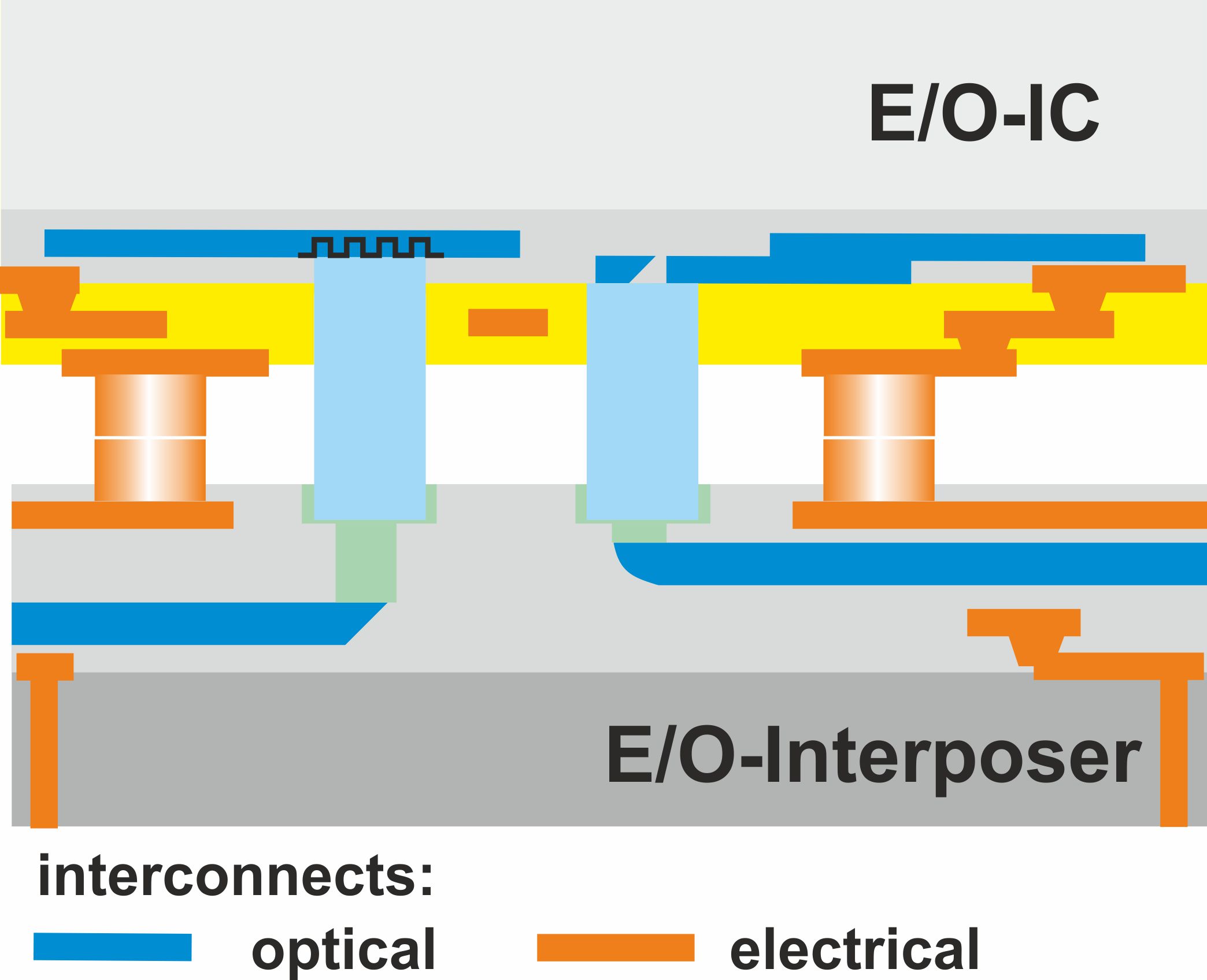
The BMBF project Silhouette (Silicon Photonics for Trusted Electronic Systems) (05/2021-04/2024) develops a platform for design, fabrication and testing of integrated photonic integrated circuits and electro-optical (E/O) interposers for photonic encryption.
With the Silhouette will our IAVT-team research on suitable packaging technologies for scalable and parallel processes of E/O hybrid integration. The focus of the investigations is on the optical signal redistribution on interposer-level and the coupling to chip-level. Direct structurable optical polymers will be used for the integration of optical waveguides and couplers, which enable an efficient and planar coupling into inorganic waveguides on chip-level (SiN-technology). The most modern waveguide materials, 3D printing and substrate processing methods as well as new multi-layer and transfer processes will be used in order to reduce the amount of process steps and thus enhance the yield for fabrication. The goal is to extend the existing technologies for fabrication of electrical interposers with optical wiring in order to integrate the optical functionality. In this regard, the compatibility of the corresponding contacting and assembly processes have to be ensured. Additionally within the Silhouette an automated testing of optical structures on chip- and interposer-level will be developed.
TU München
Deutsches Zentrum für Luft- und Raumfahrt
Fraunhofer-Gesellschaft
Wandelbots
Deutsche Telekom
atlantic labs

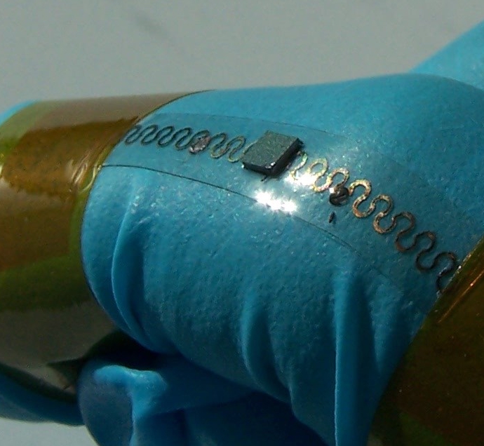
IAVT is part of excellence cluster CeTI
The “Centre for Tactile Internet with Human-in-the-Loop” (CeTI) at TU Dresden will lift the interaction between humans and robots on a new level. In future, people should be able to interact in real time with networked automated systems in the real or virtual world. In particular, humans will be within the feedback loop between the cyber and physical components of technical systems. In order to achieve this goal, various disciplines within the TU Dresden work together on this project, including electrical engineering and information technology, psychology, medicine and neuroscience. Furthermore, external partners including the TU München and the Deutsches Zentrum für Luft- und Raumfahrt and others will support the project.
The IAVT will support this research project with research on reliable flexible and stretchable electronics. The central challenge in CeTI requires sensors, such as touch and positioning sensors, as well as actuators on various positions on the body. The power supply and partially the communication between the individual elements need to be ensured by conductive tracks. Those, on the one hand need to adapt to human movements and shapes through suitable mechanical properties. But, on the on the other hand they need to keep performing flawlessly. In addition, due to the large number of different elements, a high degree of integration and miniaturization is required in order not to influence the motion sequences. Furthermore, very fast processing of the sensor signals and non-delay communication of sensor nodes between human and machine and with the network or edge cloud is required. That leads to a major prerequisite for electronic, which needs to be designed for very high frequencies.