Former public funded research projects at IAVT/ZmP
ATTENTION! The content of this page is not updated anymore!
Helmholtz-Zentrum Dresden-Rossendorf
TU Dresden, Professur für molekulare Funktionsmaterialien
TU Dresden, Institut für Halbleiter- und Mikrosystemtechnik
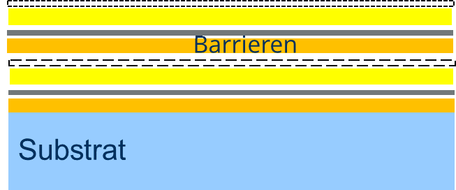
Two-dimensional (2D) semiconductors are excellently suited for sensor applications because their properties are dominated almost exclusively by their surfaces. While some 2D materials remain stable under ambient conditions, others react strongly to the surrounding atmosphere, making them inherently much more sensitive to detecting minor changes in environmental conditions. Black phosphorus—a semiconductor material with exceptionally high mobility (up to 200 cm²/Vs)—undergoes significant property changes upon exposure to ambient conditions; consequently, electronic components made from it are typically manufactured under inert gas atmospheres. This project aims to harness this material sensitivity for gas and biosensor applications while establishing a stable and selective operating environment. Selectivity poses a major challenge for sensors based on 2D materials—and black phosphorus in particular—because their high surface sensitivity typically lacks specificity regarding the species that bind to them. To achieve the necessary selectivity, the project employs a targeted approach using specialized barriers to create a selectively permeable housing environment for the sensor. As part of the project, a specialized black phosphorus-based gas sensor will be developed as a laboratory prototype. The housing environment designed for sensor encapsulation can also serve as a platform for a wide range of other sensor concepts in future projects.
First Sensor Microelectronic Packaging GmbH Dresden
viimagic GmbH Dresden
MSG Lithoglas GmbH Dresden
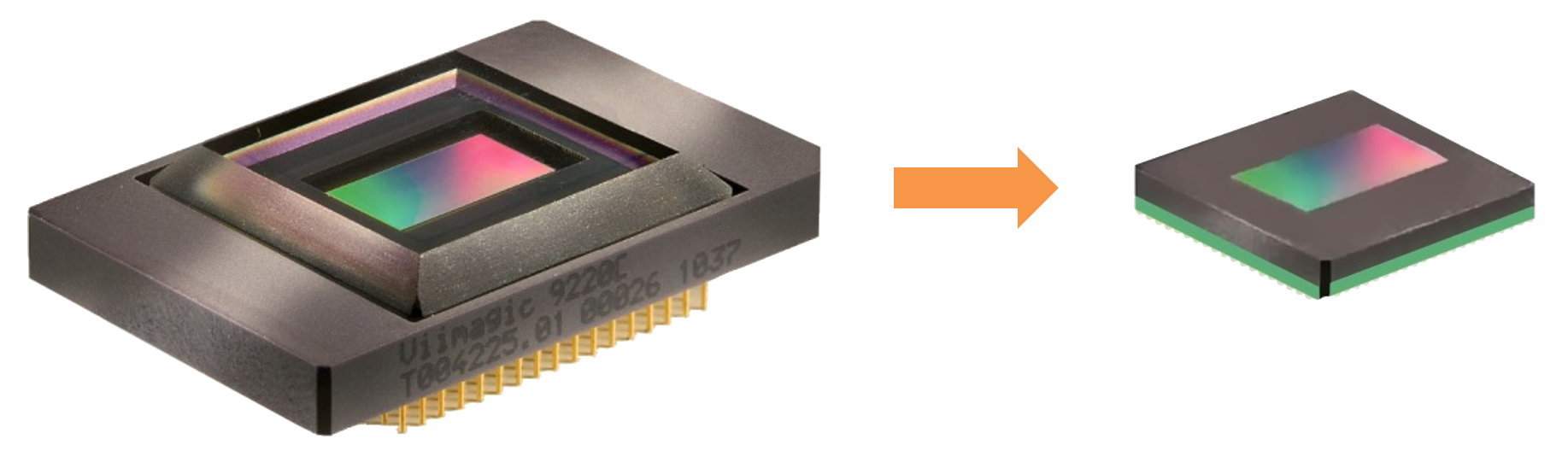

Project goal: Research and development of a new chip-on-board (COB) concept for large image sensors based on laminate substrates in a smaller form factor.
This new technology will enable the direct wafer-level mounting of cover glasses over the sensor area on the sensor chip using adhesive technologies.
A special 3D printing technology will be developed for covering the wire bridges.
TU Dresden
Based on these funding guidelines, the Federal Ministry of Education and Research supports investments at higher education institutions that possess a strong specialization in microelectronics.
The funding aims to modernize and expand research infrastructure, thereby enabling the exploration of new fields of microelectronics research at a world-class level. Furthermore, the guidelines seek to strengthen scientific exchange and cooperation among the funded institutions by fostering networking between them.
Funding is provided for investments at higher education institutions with proven expertise in the field of microelectronics. In the case of the IAVT/ZmP, the thin-film laboratory received funding for an inert-gas glovebox equipped with sputtering and evaporation systems, as well as an atomic layer deposition (ALD) system.
SITEC Industrietechnologie GmbH, Chemnitz
XENON Automatisierungstechnik GmbH, Dresden
Adenso Industrial Services GmbH, Dresden
i2s Intelligente sensorsysteme Dresden GmbH
Kontron AIS GmbH, Dresden
sunfire GmbH, Dresden
Vitesco Technologies GmbH, Limbach-Oberfrohna
Fraunhofer IWS, Dresden
ITW e.V. Chemnitz
AllMeSa's technological leadership enables the realization of systems and products worldwide through end-to-end high-performance manufacturing technologies.
AllMeSa's key technologies, encompassing mechatronic components, assemblies, and processes, participate in the growing mechatronics market (sensors, actuators, electronics).
The AllMeSa partner alliance addresses the progressively increasing complexity of products and technologies and develops the right product from its regional network of expertise.
IAVT Sub-Projects within AllMeSa
IAVT contributes to collaborative projects 3 and 4, thereby supporting the AllMeSa project components in developing novel pressure cell structuring using laser processing and glass sensors for fuel cell or electrolysis stacks.
Within sub-project 4.5, IAVT is developing a pressure/force sensor on ultrathin glass (UTG) with the goal of developing a hybrid technology on ultrathin glass as a key to high-temperature sensing.
NanoWired GmbH
Becker & Müller Schaltungsdruck GmbH
GED Gesellschaft für Elektronik und Design mbH
Huber Automotive AG
The project aims to develop a new KlettWelding-based assembly and interconnection technology and two electronic demonstrators (high-frequency data logger, high-performance DC/DC converter) based on the new Nano-AVT technology, which will meet the stringent technical requirements of autonomous driving for the first time. Replacing conventional solder joints completely eliminates the need for halogenated fluxes and reduces process temperatures by more than 80%. Furthermore, a new, full-surface, rigid connection based on KlettWelding technology will be developed to replace conventional connectors between printed circuit boards. To enable mass production of both the data logger and the DC/DC converter, a new technical interface for integrating the KlettWelding-based connections into printed circuit board manufacturing will be developed.
budatec GmbH, Berlin
Kraus Hardware GmbH, Großostheim
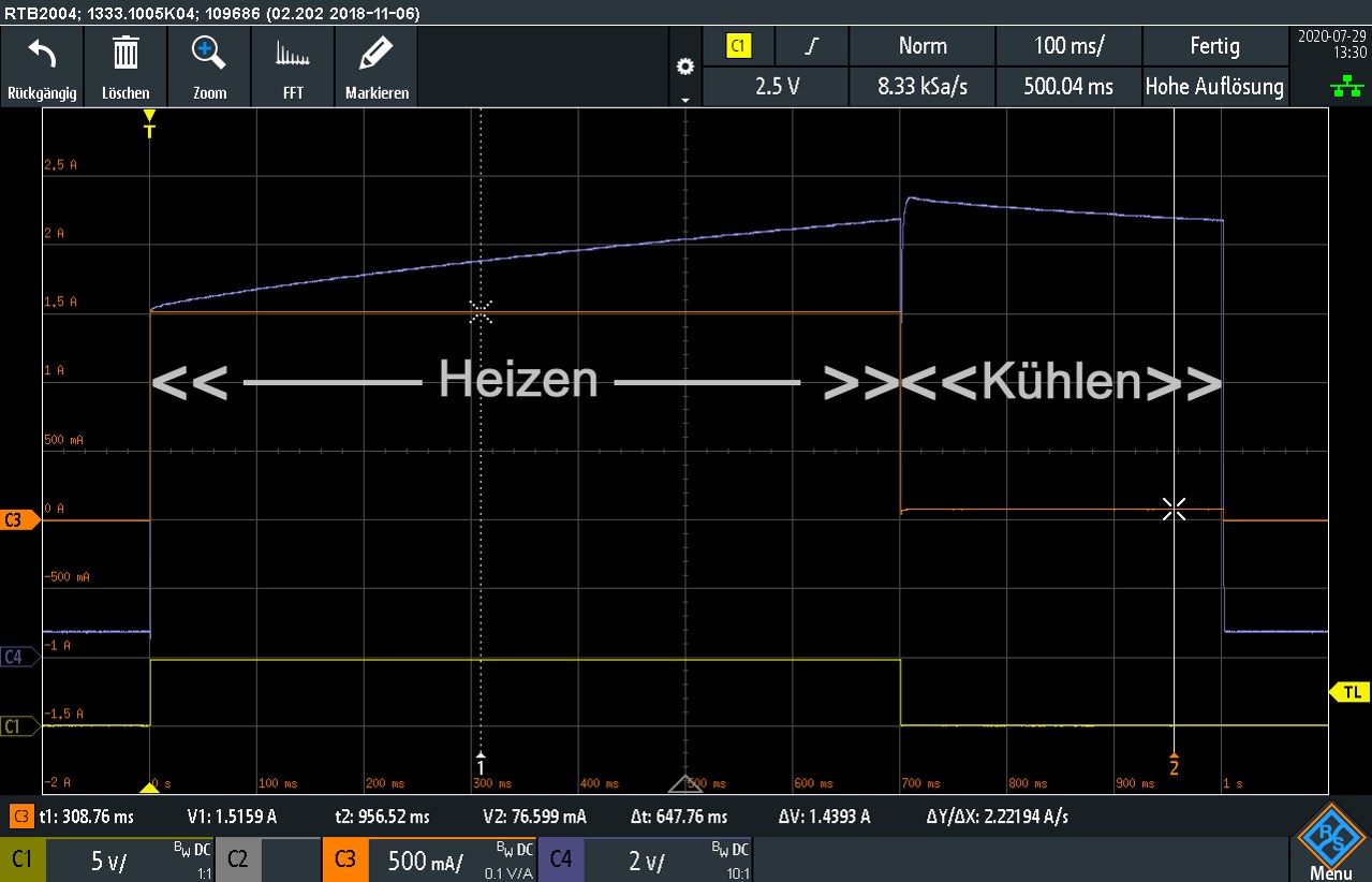
The fast and thus in-line-capable assessment of the quality of flat connection points of power semiconductors, which are produced by soldering or sintering, is a problem that has not yet been solved technically. Conventional diagnostic methods (e.g. X-ray or ultrasound microscopy) are either due to the principle or not due to the associated expenses, to carry out a direct quality control during the manufacturing process of the connection points. In the course of a previous project, a new process known as contact thermography was devised and examined in the laboratory. A miniaturized heating structure is coupled to the soldered or sintered power semiconductor as a measuring head. A short heating pulse is then introduced into the semiconductor. Depending on the quality of the connection layer underneath the semiconductor, this heating pulse spreads with different characteristics. This different propagation has a direct effect on the electrical properties of the heating structure, which can be measured. The actual measuring process (including the heating pulse) takes place within a maximum of 1 second and can therefore be integrated into the production line with absolute real-time capability. The technical implementation of the measuring principle and its integration into the process sequence in the production of power electronic modules will for the first time provide an in-line-capable test apparatus that enables real-time information on the quality of the connection points. In comparison to the previous practice of complex downstream investigations, the method promises cost-effective feasibility up to 100% testing in real time and thus direct feedback to the upstream process step of connection formation.
TU Hamburg, Institut für Flugzeug-Kabinensysteme
IMA Materialforschung und Anwendungstechnik GmbH
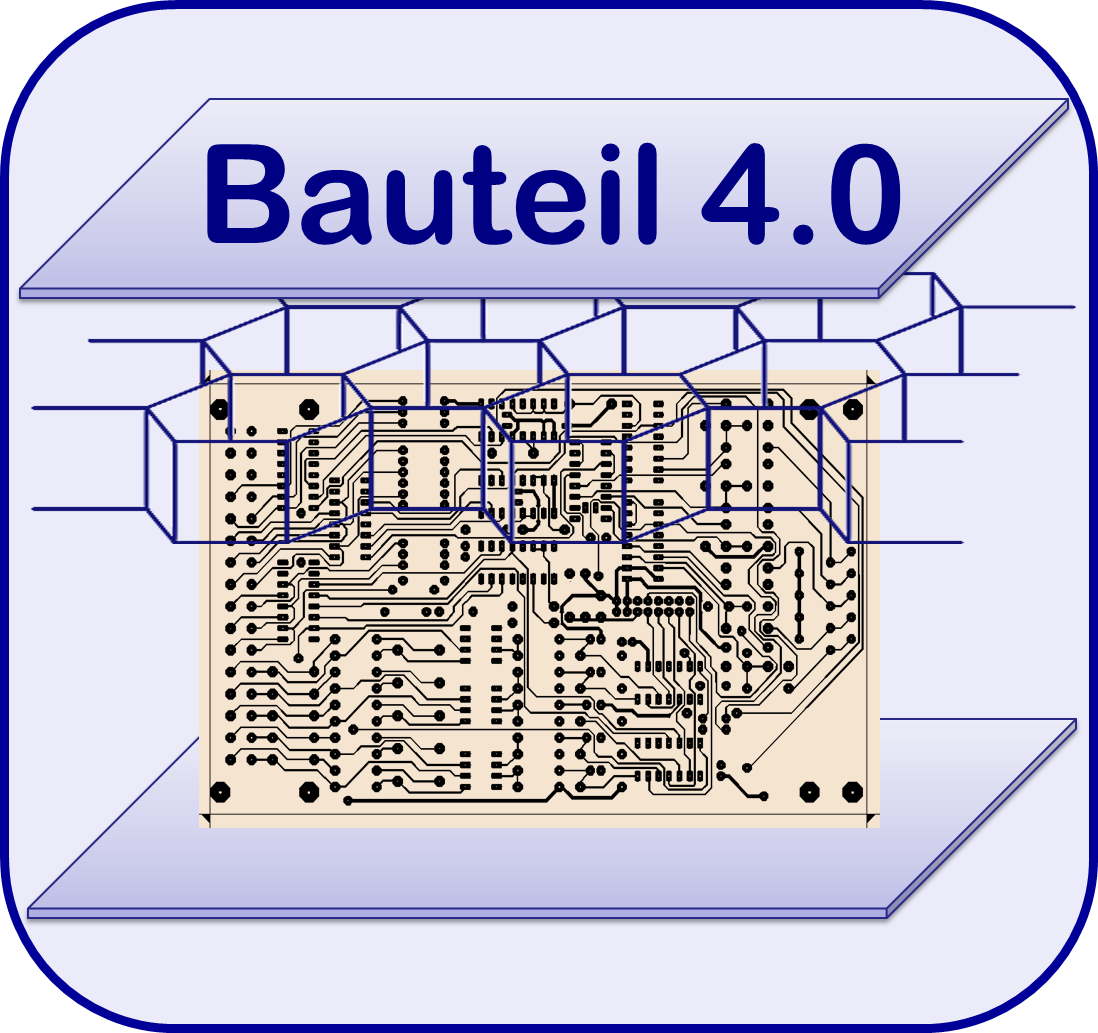
The goal of the project is the design of functions integrating, intelligtent and data processing sandwich panels for airplanes cabin - so called "Bauteile 4.0". In the past such constructional panels have been designed following strictly the convention "one function - one element". That hirarchical system and function separation restrains the ambition of developing multifunctional, highly integrated and hence weight optimized construction elements. Automotive industry has demonstrated that integration of additional functions like energy or data transfer into elements leads to wight reduction of the whole system while reliability and safety at least hold the former level. Functional integration is always combined with a plus on comfort for passengers and enables intelligent production processes as well as simplier assembly and maintenance.
Hence, there is a need in avionics industry as well to use the principle of funtional integration into elements. The airplanes cabin allows to design highly integrated elements with miscellaneous electronic and IT functions, to manufacture and implement those elements. Cabin interior, ground floor and multiple additional sndwich panels in the cabin are predestinated for that
Friedrich-Alexander University Erlangen-Nuremberg (Chair of Factory Automation and Production Systems and Institute of Optics)
Leibniz University Hannover (Institute of Transport and Automation Technology)
Laserzentrum Hannover e.V.
Current roadmaps are increasingly highlighting the role of optical bus systems as the backbone of future sensor and infotainment networks in many areas. Automotive, aerospace and industrial 4.0 applications in particular benefit from high EMC compatibility and low weight. In addition to these advantages, the high bandwidth energy efficiency and the low space requirement of optical connections are especially outstanding. In times of constantly increasing data volumes, standard copper wiring is reaching its limits, especially due to energy consumption at high transmission rates.
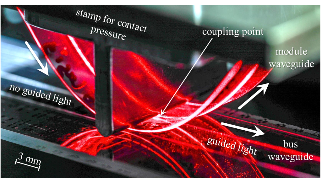
In the research group OPTAVER (Optical Packaging for 3D-optomechatronic-Devices) the modelling, simulation and additive production of polymer optical fibers on flexible foil substrates and their connection by asymmetric bus couplers as optical bus systems are investigated. In the first funding period, the system components were realized as planned and demonstrated in cooperation. The optical waveguides were first applied to a two-dimensional foil. This was conditioned in advance to improve the aspect ratio of the waveguide.
In the second funding period, the extension to three-dimensional opto-mechatronically integrated components (3D-opto-MID) is to be investigated. The formability of the thermoplastic film substrates will be used for this purpose. The three-dimensional integration of optical and mechatronic functionalities leads to an increase of the integration density and an extension of the design possibilities of opto-MID. The detachable optical couplers also offer a 3D-capable reconfigurable connection to a bus system.
budatec GmbH Berlin
Fraunhofer IKT, Dresden
LFG-Eckhard Oertel e.K, Gera
Via Electronic GmbH Hermsdorf
The project pursues the goal to improve the quality of area interconnects of power electronic modules by process integrated inspection and therefor to enhance the long-term reliability of such modules. To realize that, ceramic heating elements with high focused heating power and integrated cooling structures will be developed. A matrix of those heating-cooling elements allows an area-resolved induction of thermal energy. In addition the high dynamic behavior of the heaters allows a dedicated area- and time-resolved stimulation of the module for thermal inspection of interconnects.
Infineon Technologies Dresden and many other partners from 19 EU countries
The main objective of Productive4.0 is to achieve significant improvement in digitalising the European industry by means of electronics and ICT. Ultimately, the project aims at suitability for everyday application across all industrial sectors – up to TRL8. It addresses various industrial domains with one single approach, that of digitalisation.
What makes the project unique is the holistic system approach of consistently focusing on the three main pillars: digital production, supply chain networks and product lifecycle management.
This is part of the new concept of introducing seamless automation and network solutions as well as enhancing the transparency of data, their consistence, flexibility and overall efficiency. Currently, such a complex project can only be realised in ECSEL.
The well balanced consortium consists of 45% AENEAS, 30% ARTEMIS-IA and 25% EPOSS partners, thus bringing together all ECSEL communities. Representing over 100 relevant partners from 19 EU-member states and associated countries, it is a European project indeed.
Project Advisory Committee: Balver Zinn Josef Jost GmbH & Co.KG; Christian Koenen GmbH High Tech Stencils; Danfoss Silicon Power GmbH; DHD Deubner Hoffmann Digital GmbH Leipzig; G&W Leiterplatten Dresden GmbH & Co. KG; Hella KGaA Hueck & Co; Hensoldt; Heraeus Materials Technology GmbH & Co.KG; Microtronic Microelectronic Vertriebs GmbH; Miele & Cie. KG; Robert Bosch GmbH; Seho Systems GmbH; Sensitec GmbH; Texas Instruments Deutschland GmbH; Trainalytics; Zollner Elektronik AG
In the SMT process, it is expected that the components being processed are always flat (i.e., undistorted). In reality, however, warping and distortion occur. Standards (e.g., IPC TM 650) specify maximum values for these distortions, but these only apply to room temperature. No specific limits exist for soldering. The institute has a TherMoiré® system available for measuring the distortion of components and printed circuit boards under conditions approximating soldering. The numerous measurement results show that significant distortions occur in many components and printed circuit boards only during soldering, and these distortions correlate with real-world quality issues (e.g., head-in-pillow in BGAs) and reliability problems (e.g., pad delamination).
In this project, measurements are being carried out on various components and printed circuit boards, and the results are being compiled into a distortion database. Test boards with precisely adjustable distortion behavior are being designed. Experiments are conducted to determine the effects of such bending on quality and reliability. These reliability analyses are complemented by finite element (FE) simulations.
The final result is recommendations for more precise limits for twisting and warping, which can be incorporated into standards. This makes it possible to identify quality-critical components and derive appropriate measures (necessary measurements, design modifications, and material selection). Significant reductions in defect rates and improvements in the reliability of electronic assemblies can be expected as a result.
TU Berlin - Forschungsschwerpunkt Technologien der Mikroperipherik
Tigris Elektronik GmbH
LFG - Eckhard Oertel e. K.
The KoHLa project (miniaturised high voltage power supply for the integration in laser systems) aims for the miniaturisation and integration of a high voltage power supply used for a CO2 laser system. The power supply is a 19” rack solution as of today. A significant reduction of the size and the system integration of the power supply, innovation of electrical functionality and substrate technologies as well as new cooling approaches are focus of the project.
Using the PowerBoard technology (organic substrates with thick and structured copper trace layers) as a starting point and developing new organic-ceramic composite substrates a novel power electronics device will be developed. Replacement of recent cooling approaches, integration of analog power and digital control systems, usage of standard low cost materials and components, and the miniaturisation and system integration will be realised. Finally, a demonstrator will be manufactured showing the functionality of the power supply based on the novel technological approaches of thick copper based and organic-ceramic composite substrates.
Institut für Biomedizinische Technik der TU Dresden
Anvajo GmbH
The Technical University of Dresden (TUD) and Anvajo GmbH, a student spin-off from TUD, are jointly conducting the telemedicine project "FlexEO - Portable Device Based on Flexible Electronics and Optics for In Vivo Spectrometry of Blood Components for Telemedicine."
A portable device is being developed that can analyze blood components and parameters of the cardiovascular system outside of a clinical setting and non-invasively. The core component of the non-invasive measurement was developed over the past three years at the Institute for Assembly and Interconnection Technology of Electronics (IAVT) within the Faculty of Electrical Engineering and Information Technology (EuI): an optical microspectrometer that can decompose and analyze light into its spectral components. This microspectrometer is so small that it can easily be integrated into a finger clip or a portable device.
The microspectrometer will be embedded in a portable device that is partially based on flexible electronics. The scientists at the IAVT of TUD will design this device. Thanks to its flexible electronics, the device's sensors will be able to adapt to the wearer's anatomy. This ensures that the various sensors are optimally aligned with the body's surface. This will lead to a significant improvement in measurement quality compared to conventional methods. Novel algorithms will also take into account the pulsating blood component in human tissue. This will allow for the non-invasive determination of previously unmeasurable blood components. The necessary software is being developed within the project at the Institute of Biomedical Engineering at the Faculty of Electrical Engineering and Information Technology (EuI).
With the help of this device and its new measurement technology, conventional measurement methods will be significantly improved in terms of quality, enabling comprehensive telemedicine monitoring and care for people with chronic illnesses (such as patients with obstructive sleep apnea syndrome or diabetes mellitus) in their home environment.
GLOBALFOUNDRIES Dresden Module One Limited Liability Company & Co. KG (Gesamtprojektleitung)
HAP Handhabungs-, Automatisierungs- und Präzisionstechnik GmbH Dresden
Roth & Rau - Ortner GmbH
Institut für Technische Logistik und Arbeitssysteme der Technischen Universität Dresden
Within the Responsive Fab project, our working group is working on the sub-project "Extended Scheduling." This sub-project investigates improvement and optimization measures in the area of production planning and control, with the aim of increasing flexibility and planning stability in semiconductor manufacturing. The focus is on replacing or supplementing the current dispatching system with scheduling algorithms.
Fraunhofer Society: Institute for Photonic Microsystems (IPMS), Dresden, Institute for Electronic Nanosystems (ENAS), Chemnitz, Institute for Integrated Circuits (IIS-EAS), Dresden, Institute for Reliability and Microintegration (IZM-ASSID), Dresden; TU Dresden, Faculty of Electrical and Computer Engineering: Institute for Solid State Electronics (IFE), Institute for Electromechanical and Electronic Design (IFTE), Institute for Semiconductor and Microsystems Technology (IHM); TU Chemnitz; HTW Dresden
The center of excellence „Function integration for micro- and nanoelectronics“ is a network of facilities of TU Dresden, TU Chemnitz and the Fraunhofer Society. Its purpose is focused on strengthening the field micro- and nanoelectronics in Saxony in. A key aspect is the creation of cooperation structures between fundamental research and the needs of the local semiconductor industry. The demand of smaller, more complex and heterogeneous systems and the 3D integration of different components require a close coordination of research efforts in different fields of semiconductor manufacturing.Therefore, novel materials and processes will be investigated at the Institute for Electronic Packaging Technology. The new approaches are focused on manufacturing of micro-scale-interconnections at both lower temperatures and lower pressures and new interconnects with nanoporous intermetallic compounds.
Chair of Electrical Engines and Drives of the Institute of Power Engineering of TU Dresden
Institute of Integrative Nanosciences of Leibniz Institute for Solid State and Materials Research Dresden
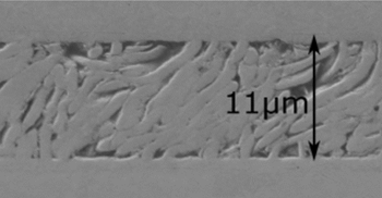
Based on the results of phase I of the DFG project and in addition to the work packages of the partners IAVT is emphasized on the development of packaging technologies for ultra thin flux sensors for magnetic fields orthogonal to the sensors plane. The complete sensor package shall have a maximum height of 150 µm including substrate, interconnection, housing and adhesive layer. Long term stability of about more than 10 years is mandatory and has to be approved by accelerated aging tests.
TU Dresden, IFE
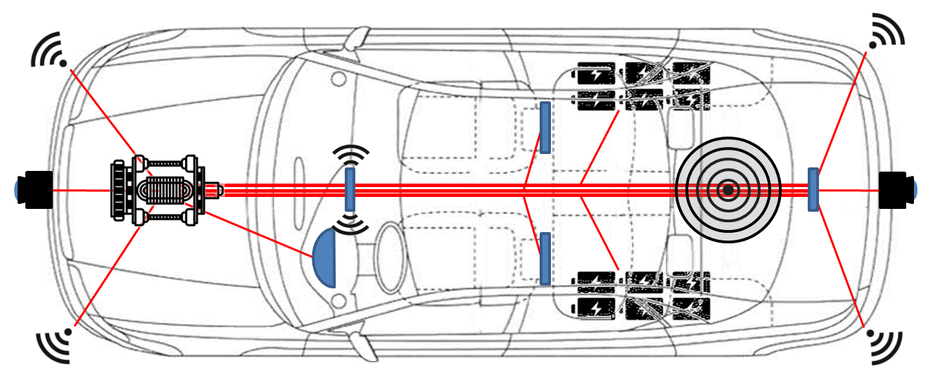
Main electronic modules indispensable for recent trends like e-mobility and regenerative energies are converters, engine control units and other power electronic modules. They contain bare power semiconductor dies out of silicon (Si) or silicon carbide (SiC) as main devices, which are mounted on the substrates using area solder joints or sintered interconnects.
One challenge using those semiconductor devices is the quality control of the interconnection with the substrate. To realize those interconnections mainly soldering is used, but more and more also sintering.
The goal of the project is to develop a cheap and finally inline capable solution for a thermography system with few pixels, that can measure the temperature distribution after thermal excitation with high temperature and time resolution as an integral across the measurement field (e.g. defined parts of the die area of a power semiconductor). The test procedure is planned as a comparing measurement, so that within a short time period (thus inline capable) the thermal transient process of the specimen can be compared with that one of a "golden part", whose interconnection quality has been evaluated in detail using laboratory methods (X-ray-tomography, scanning acoustic microscopy) or destructive testing (metallographic preparation) in detail.
TU Dresden / Institut für Textilmaschinen und textile Hochleistungswerkstofftechnik
TU Dresden / Institut für Leichtbau und Kunststofftechnik
- Process development for the implementation, integration, and contacting of both textile-based and textile-processable sensors for the precise determination of local and global stress states and damage in CFRP with thermoset matrix systems, as well as textile-processable electronic component and circuit carriers for preferably wireless signal and power transmission.
- Process instructions for the implementation and integration of the sensor systems in CFRP with minimal additional process effort for SMEs and with minimal impact on the mechanical properties of the CFRP structures.
- Realization of near-end-application functional demonstrators (e.g., CFRP load spar or wind turbine rotor blade; CFRP automotive chassis).
- Electrical insulation/shielding of the sensor systems/integrated electronic components from CFRP structures to prevent short circuits.
TU Chemnitz
FZDR Dresden Rossendorf
The Helmholtz-Zentrum Dresden-Rossendorf e.V. (HZDR), the Chemnitz University of Technology (TUC), and the Dresden University of Technology (TUD) have set themselves the goal of further developing PolCarr® technology for monitoring the adherent growth of cell cultures within the framework of the collaborative project "Development of SNEF-based touchscreens for highly sensitive, interference-free real-time control of adherent cell cultures using capacitive-electrical, inductive-electrical, and acoustic-mechanical broadband impedance spectroscopy (PolCarr-Sens)." Within the project, micro-sensors for three different, complementary broadband impedance spectroscopy methods will be integrated into microtiter plates with a PolCarr® base, and evaluation software will be developed for the routine observation of cell behavior under experimental conditions using broadband impedance spectroscopy. The PolCarr-Sens application is based on the patented PolCarr® core technology of the HZDR. PolCarr-Sens has the potential for automated high-throughput control of the properties of adherent cells and represents a significant improvement over conventional control methods, e.g., light microscopy.
Universität Rio de Janeiro
The discovery of oil in deep waters of the Pre-salt region reported some years ago by Petrobras is changing the national oil industry, requiring new technologies to be developed. Along with the challenges of marine exploitation (offshore) came the need to look for materials with increasingly specific properties to be used in submarine structures and equipment, primarily due to the severity of the environments in which these materials are operating. . In this context the steel industry has improved the development of special steels adding chromium, nickel and molybdenum contents to the basic carbon steel alloy. Due to the possible emergence of fatigue cracks and the relevance of the structures manufactured by clad steel, it is extremely important to perform periodic inspections of such equipment, and the implementation of nondestructive testing is indicated. Nondestructive tests (NDT) are tests on materials used to verify whether there are any discontinuities or internal faults in the material, without changing its physical, chemical, mechanical or dimensional features and without interfering in its subsequent use. The nondestructive technique by Eddy Current, is widely known and commonly used for structure inspection [5], because of its high capability of detecting cracks and micro cracks in various metallic materials. By operating EC devices in high-frequency (HF) and very high frequency (VHF), range (3-300 MHz [9]), capacitive effects or effect related to permittivity of the object are significantly influencing the EC signal. By interpretation of both, the conductivity and capacitive effects, a far more detailed material diagnostic becomes possible.
TU-Dresden, Faculty of Electrical and Computer Engineering:
- Institute of Semiconductor Technology and Microsystems
- Chair of Semiconductor Technology
- Institute of Telecommunications
- Chair of Radio Technology
- Junior professorship of Integrated Photonic Devices
- Vodafone chair of Mobile Communication Systems
- Deutsche Telekom chair of Communication Networks
- Institute of Electromechanical and Electronic Design
- Institute for Fundamental Electrical Engineering and Electronics
- Highly-Parallel VLSI-Systems and Neuromorphic Circuits
- Chair for Circuit Design and Network Theory
In the next 20 years, the continual miniaturization of electronics will reach its physical limits. Nowadays chips are manufactured in CMOS technology with structures less than 14 nm. The transistor geometries will decrease with further downscaling, reaching the size a few atom diameters. A promising solution is 3D-integration, the stacking of chips on top of each other. Hereby the die-stack becomes a “skyscraper” of electronics. For optimal technical usage, information must be transmit efficient through the whole die-stack. Therefore, it is necessary to analyze and develop a completely new communication infrastructure, which is both energy-efficient and resource saving.
This communication infrastructure enables a miniaturized internet within the chip-stack and therefore the young researcher scientist group calls it “3D-Atto-network”.
The microelectronic, semiconductor and photovoltaic industry has a long tradition in the area of Dresden/Freiberg/Chemnitz. The topic of this young researcher group is one of the most important for the future information and communication technology industry in Saxony and Germany (see high tech industry of the German Confederation and the Free State of Saxony). The Saxony research and development cluster “Silicon Saxony”, including around 300 companies and 40.0000 employees, which has recognized its importance, also supports it.
The 3D-Atto-networks that are based on 3D-integration will become a key technology for future products, innovative technologies and megatrends as Smart Cities, Smart Grids or Industry 4.0. Including for example the tactile internet and the 5G mobile phone standard launched in around 2022.
All partners of the CRC belong to Technische Universität Dresden.
Faculty of Electrical and Computer Engineering:
- Institute of Principles of Electrical and Electronic Engineering
- Institute of Communications Technology
- Institute of Electronic Packaging Technology
Faculty of Computer Science:
- Institute of Computer Engineering
- Institute of Systems Architecture
- Institute of Software and Multimedia Technology
- Institute of Theoretical Computer Science
Faculty of Natural Science, Mathematics Section
- Institute of Numerical Mathematics
Center for Information Services and High Performance Computing (ZIH)
Sub-Project A10: System integration for optical and wireless Pbit/s communication in high performance computing
Addressing the increasing energy demand of global internet usage and the resulting ecological impact of it, the visionary goal of the collaborative research center HAEC (“Highly Adaptive Energy-Efficient Computing”) is to research technologies to enable computing systems with high energy efficiency without compromising on high performance. To achieve the goal of an integrated approach of highly adaptive energy-efficient computing, the problem is approached at all levels of technology involved, the hardware, the computer architecture and operating system, the software modeling as well as the application modeling and runtime control levels. A novel concept (HAEC box) of how computers can be built by utilizing innovative ideas of optical and wireless chip-to-chip communications shall be explored. The HAEC collaborative research center is a first attempt to achieve high adaptivity and energy efficiency with an integrated approach.
In the CRC 912 the IAVT works on the project A10: System integration for optical and wireless Pbit/s communication in high performance computing. The main research focus of the project is the integration of components of communication transceivers into the high performance package. In the phase II following research areas are investigated: electro-optical integration on board- and package-level, packaging for mm-wave communication and embedding/integration of link components on the wafer-level.
Friedrich-Alexander University Erlangen-Nuremberg (Chair of Factory Automation and Production Systems and Institute of Optics)
Leibniz University Hannover (Institute of Transport and Automation Technology)
The potential of precise space-resolved strain measurements or the capacity to transmit very large amounts of data are two examples of the beneficial use of optical systems. Apart from the general advantages of the optical signal line, like as far as possible immunity to electromagnetic radiation, being non-sparking for the use in potentially explosive areas or the low weight compared to copper cables, modern technologies make use of the possibilities to integrate optical waveguides into structural components. Questions regarding the integration of optical waveguides into fiberglass composite components or into printed circuit boards are, among others, the subject of current research.
However, questions regarding the signal transfer at nods in photonic networks are still unsolved. There are possibilities of optical-electrical and electrical-optical signal conversion. Though an exclusively passive coupling of optical signals is currently subject to restrictions. This and other challenges of the optical assembly and interconnection technology are picked up by the dislocated research group.
The goal of the dislocated research group is to research methods and technologies for the design, construction and manufacturing of three-dimensional optically functionalized mechatronic components (3D-opto MID).
Job Thermo Bulbs GmbH Ahrensburg
Thermo bulbs are thermal sensitive trigger trigger elements for sprinkler systems, fire flaps and other elements. The latest JOB development is the so called "Extinguishing Bulb (E-Bulb)" for fire extinction in electrical circuits. Bursting of the glas ampulla at a defined temperature level a non-conductive and non-toxic fluid is evaporated which immediatly becomes gaseous. The cooling effect and the eliminating of oxygen the fire is extinguished within seconds. This concept together with an electrical functionalization of the thermo bulb shall be developed further. In addition to the passive triggering based on the environmental temperature the newly develeoped EF-Bulb shall also be triggerable actively by heating up the bulb and such initializing the bursting. With such triggering mechanism new application field in fire protection can be developed with increased triggering sensitivity and reduced reaction time.
BBAA Berlin Brandenburg Aerospace Allianz e.V., Hamburg Aviation - Luftfahrtcluster Metropolregion Hamburg e.V., Kompetenzzentrum Luft- und Raumfahrttechnik Sachsen/Thüringen e.V., Silicon Saxony Management GmbH
The general goal of the project is an improved networking between stakeholders in the field of aviation and space flight. It's especially emphasized on an improved interaction between suppliers and service providers of semiconductor and electronic industry on one side and specific module suppliers (Tier1, Tier2, etc.) and system manufacturers (OEM) of aviation industry on the other side.
The project part of TU Dresden is focused on "integration concepts for muliti functional components in the special environment of aviation industry". The special contribution of this part is the systematic analysis of research topics of the involved cluster regions as well as on an international level. The main focus is about the application of innovative technologies of electronics packaging in avionics, especially in the field of cabin systems.k.
TU Dresden / Institut für Textilmaschinen und textile Hochleistungswerkstofftechnik, Technische Universität Clausthal / Institut für Polymerwerkstoffe und Kunststofftechnik
The aim of this research project is to further develop the high-frequency eddy current method into a flexible, process-integrated, and automated quality assurance method suitable for SMEs in the production of textile carbon fiber-based semi-finished products and preforms, the impregnation process, and cured CFRP components. This development aims to create a basis for the automatic detection, identification, and quantification of defects and quality deficiencies along the entire CFRP manufacturing process chain using eddy current measurement technology. Due to its particular technological and economic relevance for SMEs, this development will be carried out using the processes of multiaxial warp knitting (semi-finished product manufacturing), binder forming technology (preform manufacturing), and vacuum infusion (composite manufacturing).