Services and Equipment
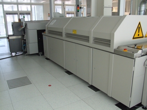
Manufacturing, Assembling, Treatment

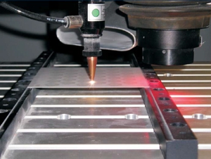
Printed Circuit Boards and Printing Masks
Printed Circuit Boards and Printing Masks
Services
- Manufacturing of Herstellung von phot masters for PCB production
- Manufacturing of one-sided, double-sided and multilayer PCBs (up to 6 layers) including through hole metallization
- Manufacturing of copper printing masks by etching
Equipment
- Equipment for manufacturing of PCBs and printing masks
- Computer controlled mill-drill-plotter Bungard CCD, maximum rotation speed 60.000 rot./min, drilling diameter 0.3 - 4 mm
- PCB brush engine, Bungard
- Galvanic Compakta for tenting technology, Bungard, maximum workpiece size 300 mm x 400 mm
- Etching machine, Bungard, copper-II-chloride
- Stripper sodium hydroxide
- Rigid resist laminators (Hot rol), Bungard
- phot. etching resist 40 µm, width 300 mm
- phot. solder mask 65 µm, width 400 mm
- Exposurer, Bungard EXP 8000
- Multi layer laminator MLP 20

Thick Film Technology
Thick Film Technology
Services
- Testing of new materials and development of technologies
- Prototyping and manufacturing of examples
- Characterization of thick film components and layer systems
Equipment
- Mask preparation
- photo plotter (Gerber format)
- screens with emulsion (steel and polyester canvas, standard / fine)
- copper masks (double sided etched)
- steel masks (laser cut)
- Laser technology
- drilling of vias in ceramic substrates and polymer foils
- cutting and scribing of outlines for panel separation
- resistor trimming
- Screen printing technology
- MPM-SPM (with vision system)
- EKRA X5 STS
- Sintering technology
- programmable batch furnace ATV PEO 603
- zone furnace BTU up to 1100 °C
- Possible technologies
- CERMET thick film technology on Al2O3-ceramics
- Low Temperature Cofired Ceramic Technology – LTCC
- Polymer thick film technology on organic flex substrates


Prototyping and Module Assembly
Prototyping and Module Assembly
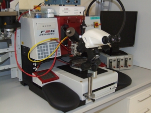
Multi-head wire bonder 56xx
SMD assembly line (stencil printer, component placement, convection soldering)
Services
- Assembly of electronic modules, prefered in SMD technology
- First- and second-level interconnect technologies
Equipment
Micro assembly:
- Ultrasonic and thermosonic wire bonder F&K Delvotec 54xx and 56xx
- Flip chip bonder
- Fineplacer
Application of interconnect materials:
- Mask printing equipment EKRA X3
- Dispensing machine Martin
Placement of components:
- SMD-assembling machine SIPLACE SX1
- SMD-aasembling machine Fuji NXT-II
- Places for manual assembly
Soldering technologies:
- Convection reflow soldering equipment Rehm V8 2.1
- Wave soldering equipment Seho GoWave
- Vapor phase soldering equipment IBL
- Rehm Condenso XM
- Selective soldering equipment (light) ATN economic A400


Laser treatment of materials
Laser treatment of materials
Laser station
Services
- Material treatment of ceramics and thin metal foils
- Thick film resistor trimming
- Drilling and cutting
- Laser soldering
- Laser micro welding
Equipment
- 3D-Micromac microCUTms10.6: CO2 laser, 200 W + fibre laser, power 20 W
- Welding laser LSW 4001
Measuring

Geometrical characterization
Geometrical characterization
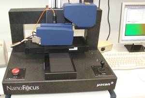
3D profiling NanoFocus µscan with different sensors
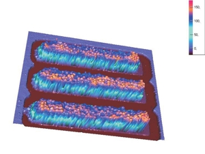
Measurement of a printed solder volume
Services
- contact-free topological measurement of surfaces
- determination of roughness
- volume calculation
- needle-contact topoligical Measurement of surfaces
Equipment
- Laser profilometer NanoFOCUS µScan AF2000
- Measurement system NanoFOCUS µSurf
- NanoFOCUS µSprint
- MarSurf CP select
- 3D-coordinates measurement equipment PMC 500
- Two-coordinates Measurement microscope ZKM 01-250C (Carl Zeiss)
- Bruker DektakXTA

Dynamic Topography Measurement
Dynamic Topography Measurement

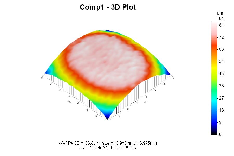
BGA topography @ 245°C
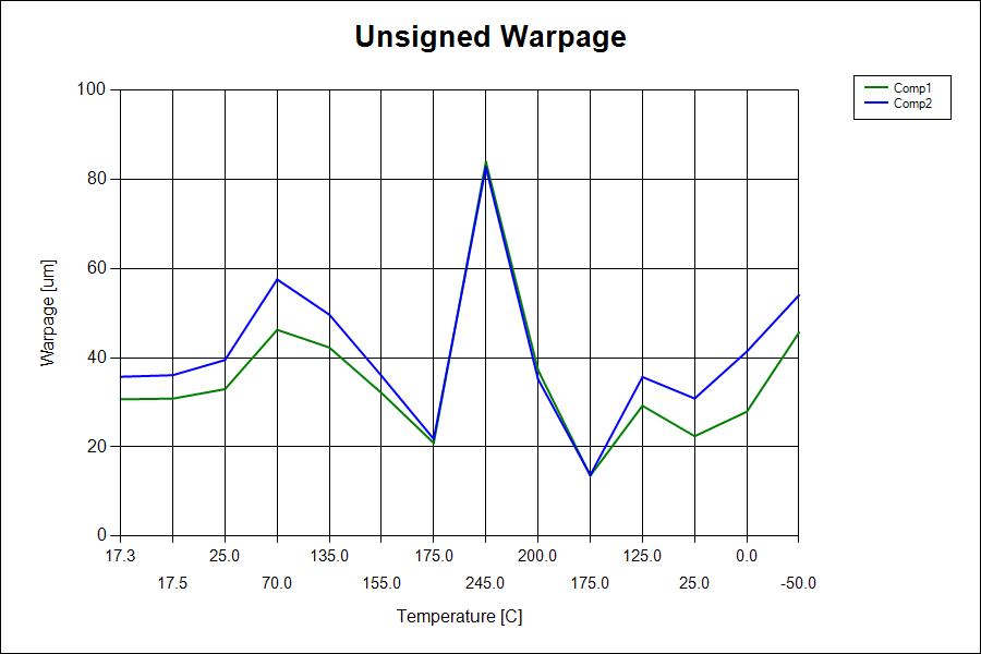
Coplanarity mismatch, unsigned
Services
Measurement of topography and deformation and its changing on flat objects under changing temperature conditions (e.g. simulation of soldering temperature profile up to 280°C, temperature cycles down to -50°C)
Sample objects:
- bare Printed Circuit Boards
- components (BGA, LGA, QFP, QFN)
Sample objects which need special preparation:
- SMD connectors
- assembled PCB
other objects on request (please deliver object pictures and dimensions before)
Equipment
- Insidix TDM Compact II
- Objects up to (300 x 200) mm2
- Infrared heating (max. temperature gradient 3K/s)
- Active cooling (max. temperature gradient -3K/s)
- Temperature range: -50°C ... 300°C
- Accuracy z-direction: 1,5 µm repeatabilityt
- Resolution vs. measurement area (FOV = Field of View)
- 53 µm @ (195 x 155) mm²
- 31 µm @ (110 x 90) mm²
- 10 µm @ (37 x 30) mm²
- 3 µm @ (12 x 10) mm²


Physical characterization
Physical characterization
Rheology
Services
- Determination of rheological behaviour of pastes
- Investigation of the influence of surface treatment, in example on the releasing behaviour of printing screens and masks
Equipment
- Rheometer HAAKE RheoStress 600
- VC Motor controlled
- mimimum torque 0.5 µNm
- angle resolution of 0.012 µrad
- Peltier-tempered plate-conus-system
- T=(-60 – 185) °C
- Measurement in three modes:
- shear stress presetting (CS-mode)
- rotation speed presetting (CR-mode)
- deformation-controlled (CD-Modus)
- VC Motor controlled
Contact angle measurement
Services
- Contact Angle measurement
- Calculation of surface tension and surface energy of packaging materials
- Statistical analysis and failure analysis
Equipment
- Contact angle measurement equipment dataphysics OCA 20

Analyze

Scanning acoustic microscopy
Scanning acoustic microscopy
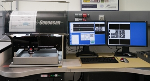
Scanning acoustic microscope
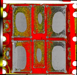
Failure detection in DCB modules
Service
- Non-destructive inspection of prototypes and samples of packaged and unpackaged components, devices and substrates.
- Layer by layer detection of failures like delaminations, gas inclusions, cracks and selective micro defects, especially of laminates, large area adhesions (e.g. heatsinks) and DCB substrates.
- Run-time analysis to describe material inhomogeneity.
- Ultrasonic scans are documented as files or color printed images.
Equipment
Ultrasonic microscope SONOSCAN C-SAM® Gen6™
- Changeable transducers with the following frequencies and lateral resolutions:
- 10 MHz: 250 µm
- 15 MHz: 175 µm
- 20 MHz: 125 µm
- 30 MHz: 75 µm
- 50 MHz: 50 µm
- 60 MHz: 30 µm
- 100 MHz: 25 µm
- 230 MHz: 10 µm
- Investigation depth up to some millimeters depending on the frequency and the material
- Investigation methods C-Scan, Q-BAM™, THRU-Scan™
- VRM™ (complete storage of echo signals of the specimen), regenerating of defect images of any layer, extraction of three-dimensional information, run-time topography
- Coupling medium: de-ionised water

X-ray diagnostics
X-ray diagnostics
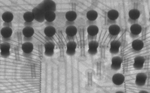
Radiography of BGA solder joints using oblique view
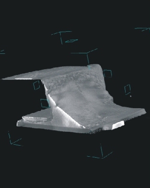
Volume model of a tomography of a passives solder joint
X-ray radiography
Service
Equipment
- Non-destructive inspection of electronic devices and modules, especially with high contrastive materials (solder, metallisation), e.g.:
- Standard- and fine-pitch-SMT and THT solder joints
- BGA-, COB-, CSP- and Flip-Chip solder joints
- Missing and imperfect solder joints
- Displacement
- Shorts
- Solder joint analysis (voids)
- Multilayer PCB
- X-ray microscope phoenix|x-ray nanome|x
- high resolution vertical or oblique view up to 70°
- high resolution real time image processing or alternatively digital detector
- CCD camera: 1126 x 1600 pixel, resolution 12 bit
- Digital detector: 1000 x 1000 pixel, resolution 14 bit
- geometrical magnification: > 1.000 times
- minimal detail visibility: 400nm
X-ray Computer Tomography
Services
- Volume analysis and reconstruction of electronic devices and modules
Equipment
- X-ray Computer Tomography equipment nanotom
- open nanofocus tube with tungsten target
- acceleration voltage: 10 – 180kV / 15W
- beam current: 5 – 1.000µA
- precision manipulation on a granit base
- high resolution digital detector with 2.400 x 2.400 Pixel, 12 bit
- pixel size: 50µm x 50µm
- minimal voxel size: < (500nm x 500nm x 500nm)
- geometric magnification: 1,7-times to 1.000-times
- maximal specimen size/ weight: h = 150mm, d = 120mm, m = 1kg

Metallographic preparation of packages
Metallographic preparation of packages
Services
- Preparation of a target layer
- Analysis of microstructures, cracks, delaminations and voids (e.g. for packaging qualification after thermal-mechanical stress)
- Measurement of structure size, like intermetallics, lengths, layer thicknesses
- Documentation and reporting of the results
Equipment
- Grinding and polishing: TegraSystem (TegraForce-5, TegraPol-35)
- Precision sectioning saws: IsoMet 1000 (bis 1000 RPM), Accutom-2 (3000 RPM)
- Microscopy: Leica DM4000 M (max. magnification 1000x) and digital camera (2080x1544 pixel)
- Reflected light methods: bright field, dark field, polarized light, differential
interference contrast
- Reflected light methods: bright field, dark field, polarized light, differential
- Database image management system


Storage testing, accelerated aging
Storage testing, accelerated aging
Service
- Temperature profile detection
- Off-line measurement
- On-line measurement
- Zero-Ohms resistance measurement
- Failure detection with defined shut down of cycle chambers
- Voltage measurement
Equipment
- Temperature test chamber
-
- Single chamber system Feutron TPK 600
- Temperature range: -70 °C to 180 °C
- Temperature gradient: 10K/min (-55 °C to 150 °C)
- Power cycle chamber
- Two chamber system Feutron TSK 200
- Hot chamber: 10 °C to 200 °C
- Cold chamber: -75 °C to 180 °C
- Zerol-Ohm measurement system
- Four-point resistance measurement
- Software controlled
- Temperature triggered
- Keithley-Delta-Mode System
- Nano volt meter Keithley Modell 2182A
- Current source Keithley Modell 6121
- 128 channel multiplexer
- Voltage measurement
- Four-point resistance measurement
- Isothermal storage
- Temperature range: -80 °C to 300 °C

Note
Additional information about equipment and services and how you can use it can be found following the links below