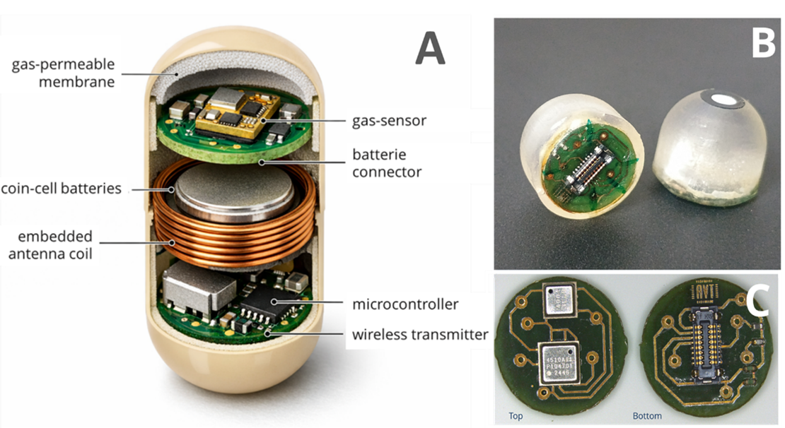


The ongoing trend toward the miniaturization of electronic components is also opening up new fields of application for sensor technology. Particularly in biotechnological and medical systems, severely limited installation space, for example in implants, represents a key boundary condition for system integration. The fabrication of sensors using semiconductor manufacturing processes enables significantly increased integration densities and reduced production costs for miniaturized sensor systems.
These systems pose particular challenges for conventional chip assembly and interconnection technology, as sensor packaging is not solely focused on protecting electronic components. In contrast to power devices or information-processing ICs, sensor systems usually have to interact with their environment in a defined manner. For the detection of chemical, biological, or physical parameters, a defined exchange of substances with gases, liquids, cells, or biomolecules is required. Complete encapsulation using established standard processes such as transfer molding is therefore unsuitable in many cases. Sensitive layers must remain selectively exposed, whereas conductor tracks, contacts, and readout electronics must be reliably protected against moisture, corrosion, and ion migration. This results in stringent requirements for selective passivation, interface stability, material selection, and process control.
In addition, electrochemical sensors and biosensors frequently employ functionalized surfaces, such as enzyme, hydrogel, polymer, or nanomaterial layers. These layers are often thermally, chemically, and mechanically sensitive and require material- and function-preserving processes for electrical contacting, assembly, and integration. Conventional assembly and interconnection processes must therefore be adapted or supplemented by low-temperature and material-compatible technologies. For applications in medical and biological environments, biocompatibility of all materials used is also of central importance. Substrates, metallization, adhesives, passivation layers, and packaging materials must not induce cytotoxic effects or undesired biological reactions.
The IAVT addresses these challenges in research and development projects along the entire process chain of sensor packaging. In this context, we develop application-specific solutions ranging from low-temperature and material-preserving contacting processes to selective passivation concepts and semipermeable encapsulations for defined mass transport. In addition, research is currently focused on the development of packaging and integration concepts for sensors in robust ceramic-based electronic systems.