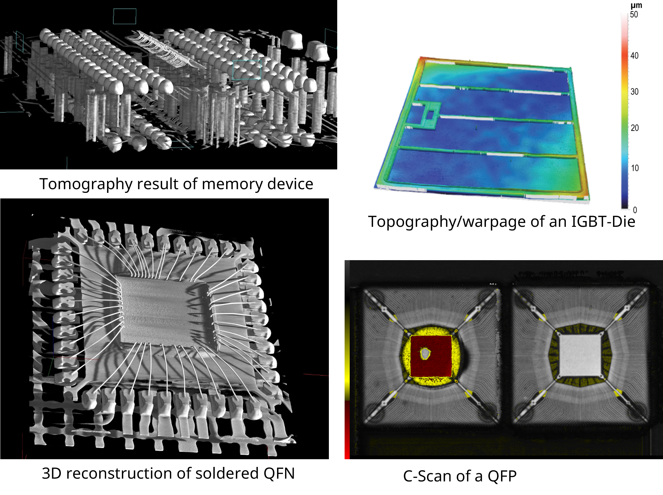


Verifying the performance of new, typically miniaturized, technological solutions in electronic packaging requires suitable, ideally non-destructive, testing methods. A major challenge for these testing procedures is the wide variety of materials employed, each with distinct physical, chemical, and technological properties. Another crucial aspect of non-destructive testing is the analysis of damage mechanisms and the interpretation of defect patterns.
High-resolution geometric measurement of substrates and components is also a key component of non-destructive testing.
To address these requirements, the IAVT/ZmP is equipped with state-of-the-art systems for X-ray inspection (radiography, laminography, CT), scanning acoustic microscopy, and optical surface characterization. Furthermore, the field of diagnostics and characterization encompasses exploring new applications for standard techniques and developing novel methods for image reconstruction and signal processing, such as researching and applying artificial intelligence (e.g., using neural networks for defect detection, transfer learning, and deep learning).
We make our expertise in diagnostics and characterization—covering both individual components and assembled units—available to industry partners through the joint "nanoeva - Competence Center for High-Resolution Non-Destructive Testing," operated in collaboration with Fraunhofer IKTS.