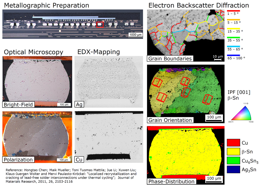
Peter Haasen defines „microstructure as all the existing lattice defects in a metal which are not in thermodynamic equilibrium (according to type, number, distribution, size and shape)” [1]. If activated (e.g. by increased temperature during operation) these crystal defects can form undesirable changes in microstructure which affect the mechanical and electrical function. Apart from that, it is also necessary to investigate material interactions (such as interdiffusion or corrosion). In addition, the microstructure analysis is relevant to the examination of technological processes which makes it an important tool for process optimization.
[1] Haasen, P.: Chapter 3 – Microstructure and Phase, Grain- and Phase Boundaries“, In: Physical Metalurgy, 3rd Revised Edition, Cambridge University Press, 1996, S. 42, 978-0-521-55925-6 (ISBN)
Microstructure characterization and its methods will remain one of the most important process-related tools for the implementation of future technologies, and the use of new materials for electronics packaging. Moreover, it is an integral part of the physics of failure analysis for existing and future solutions in electronics packaging.