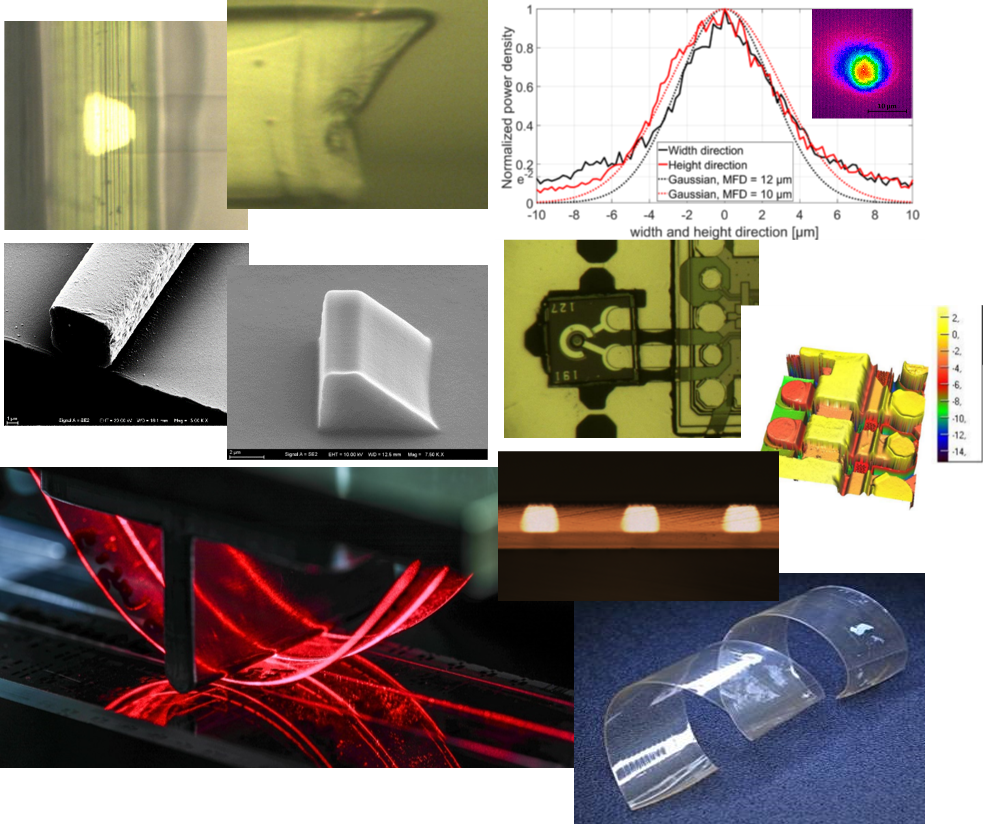
The continuously increasing bandwidth and energy efficiency demand requires alternatives to electrical interconnection technologies at printed circuit board (PCB) and interposer level cost-effective. Being well established in telecommunication, the optical interconnection technology exhibits advantages in electro-magnetic compatibility, power dissipation, layout and weight here too. Future substrates will be hybrids that combine electrical and optical interconnections. Our research group “Optical Interconnects and Packaging” is dedicated to technology development for the fabrication and integration of optical waveguides for the PCB and interposer level, investigates process compatibility as well as reliability and researches on coupling concepts between integrated single- and multimode waveguides and optical transmitters or receivers.
Already several times the conventional copper-based interconnection technology has demonstrated specifications beyond previously perceived technical limits. The bandwidth reserve by itself will not be sufficient to initiate the paradigm shift towards optical interconnections. Only if cost effective technologies exist a step-by-step transition will take place. To make this happen low-loss materials with increased thermal stability and compatible fabrication technologies for integration of waveguides and coupling optics have to be developed. Optical interconnection technology also defines new demands for the manufacturing regarding the grade of cleanliness, assembly tolerances and test procedures. The key issue will be the development of efficient coupling strategies that preferably allow for passive alignment and surface mount technology. These requires further development of packaging technologies for scalable and parallel manufacturing processes of electro-optical (E/O) hybrid integration aiming at decrease of process steps and complexity. Complex hybrid E/O-substrates can be only developed if design software addresses specific design rules and is enhanced by simulations.
Tasks for academic work and ongoing projects can be found under the following links: