The on-going miniaturization (increase in the integration density) of electrical contacts in packaging technology and the complexity of the material systems used (hetero-integration, interface problems) place very high demands on the processing (low-temperature and low-pressure connection technologies), on the heat dissipation (especially when stacking chips vertically) and the reliability (new materials, interfaces, CTE mismatch, etc.) of the technologies used. In the long term, these requirements shift the focus of packaging to the nanometer range, since nanomaterials and nanostructured surfaces enable both optimized material properties and the desired scaling.
The most important topics in the field of technology are:
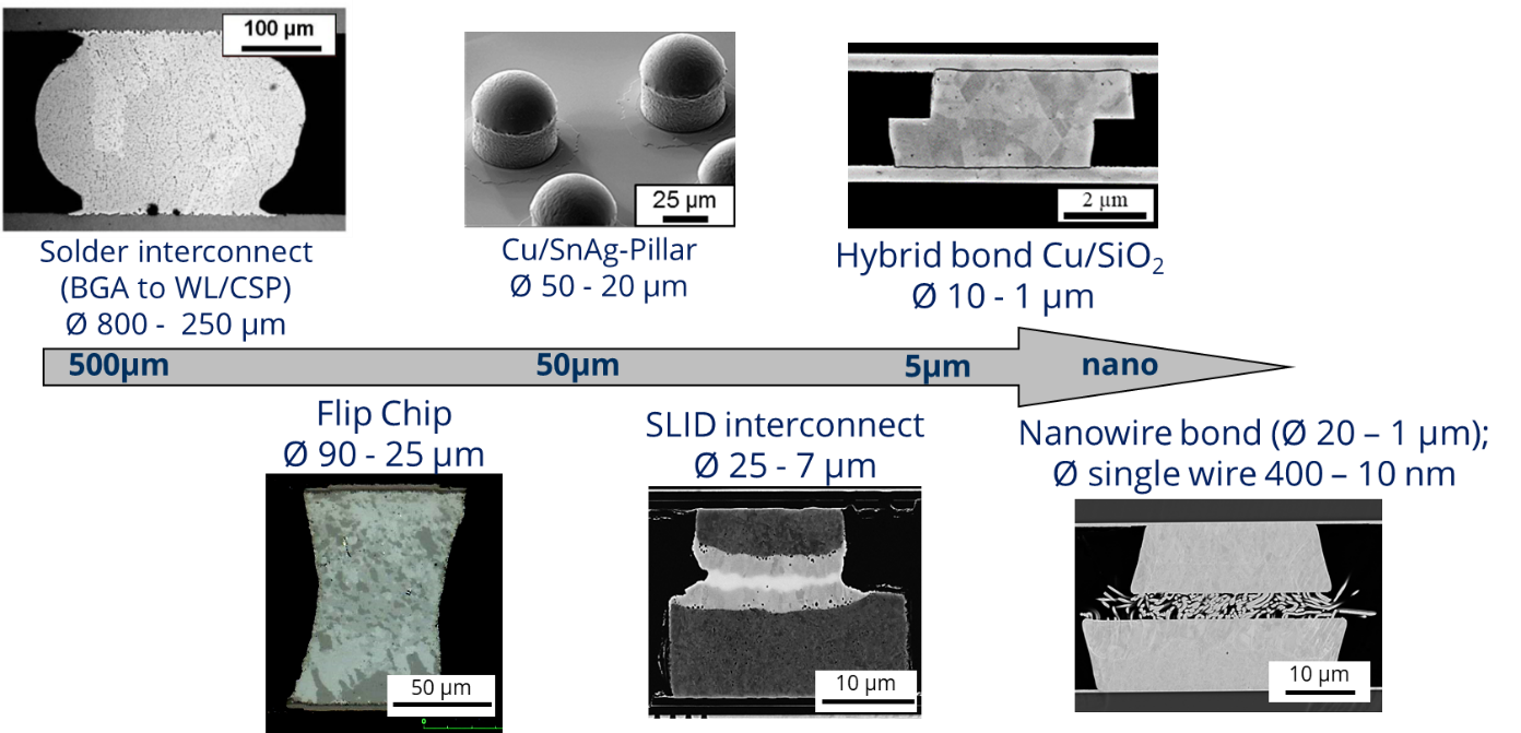
- Solid Liquid Interdiffusion (SLID) microcontacts with Sn, SnAg, Cu, In, Ni;
- Cu/Cu diffusion junctions with self-assembled monolayers (ultrasound flip-chip bonding);
- Hybrid bond contacts with Cu and SiO2;
- Polymer-based contacts for chip sealing;
- Electroplating of In as a solder material for micro-contact applications;
- Inspection methods (metrology) for micro-contacts;
- Nanowire-based Cu/Cu micro-contacts.
In the field of analysis we deal with the following topics:
- Characterization of intermetallic phases in solder and SLID contacts (kinetics, structure analysis, corrosion);
- Research about causes of the formation of nano-porous SLID contacts;
- Accelerated aging / reliability tests for micro contacts (e.g. SLID and hybrid bond contacts);
- Mechanical strength of SLID, Cu/Cu and polymer-based contacts;
- Characterization of galvanic copper layers and solder layers as well as orientation analysis with EBSD;
- Analysis of the process influences on the microstructure of lead-free solder materials.